PCB Via-Stitching Thermal Solver
Calculate the effective vertical thermal conductivity through a PCB stackup with via stitching, and estimate temperature rise for a given heat load.
PCB Geometry & Materials
Copper layers 2
Copper thickness L1
mm
mil
oz
Copper thickness L2
mm
mil
oz
Total PCB thickness
mm
mil
Dielectric thermal conductivity
W/m·K
Via Parameters
Via drill size
mm
mil
Via plating enabled
Via plating thickness
mm
mil
Via stitching pitch
mm
mil
Via fill enabled
Via fill thermal conductivity
W/m·K
Component & Heat Load
Component width
mm
mil
Component length
mm
mil
Heat dissipation
W
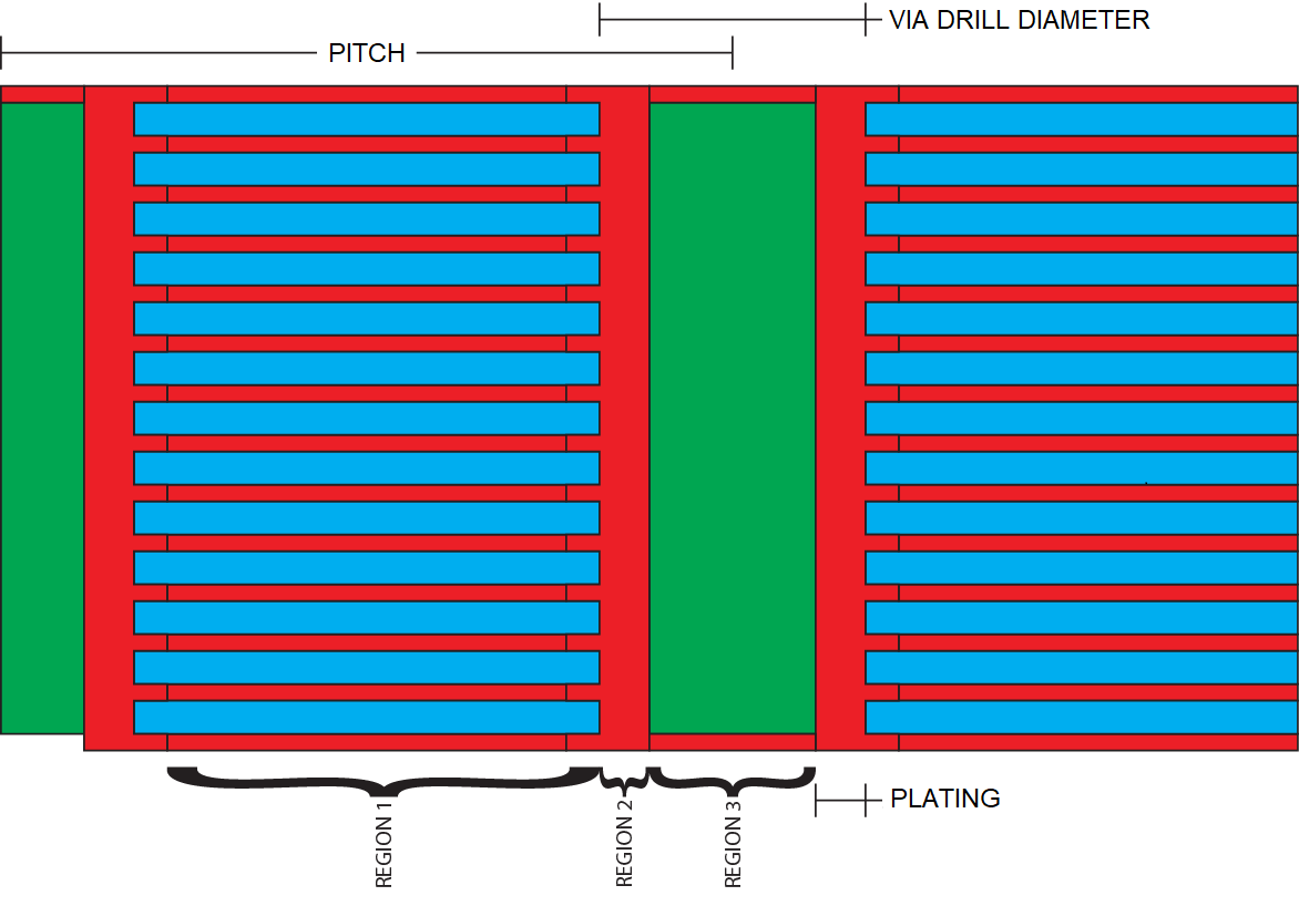
Effective Through-Plane Conductivity
Computed dielectric thickness 1.5052 mm (59.26 mil)
Region 1 k (PCB stackup) 0.262 W/m·K
Region 2 k (via plating) 401.0 W/m·K
Region 3 k (via fill/void) 3.000 W/m·K
Area fraction Region 1 87.434%
Area fraction Region 2 2.989%
Area fraction Region 3 9.577%
Total effective k_through 12.503 W/m·K
PCB Temperature Rise
ΔT across PCB 19.681 K